What RF simulation needs from your eCAD file
The geometry of your PCB design has a significant impact on how smoothly your RF simulation will run, both in terms of setup and result accuracy.
To help you prepare an efficient and simulation-friendly model, we’ve outlined the key elements your eCAD file should include. Following these guidelines will help you ensure a clean, reliable geometry for your CENOS RF simulations.
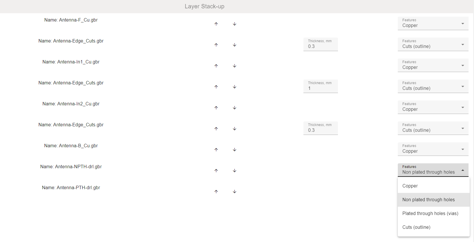
Files needed
For CENOS RF simulations, you only need a few specific layers from your eCAD design:
- Copper Layers: Top and bottom copper (or more, if simulating multilayer boards).
- Board Outline: The mechanical boundary of the PCB.
- PTH (Plated Through Holes): For vias or through-hole pads that affect the RF signal.
- NPTH (Non-Plated Through Holes): For mechanical holes that are not electrically conductive.
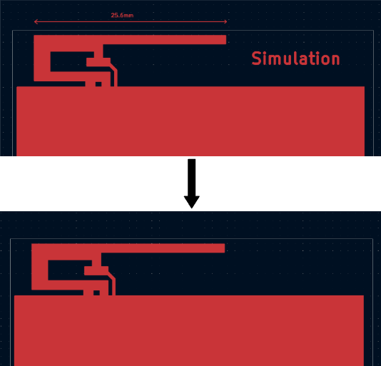
Optimize your design
Many PCB designs contain layers and details that are irrelevant to electromagnetic simulation. Cleaning up your file before importing it into CENOS helps reduce simulation time, improves stability, and ensures more accurate results.
Why optimize your eCAD file?
- Faster simulations: Removing unnecessary details reduces mesh size and speeds up computation.
- Focus on relevant physics: Many layout details (e.g., silkscreen, vias not involved in the RF path) don’t affect RF performance and can be omitted.
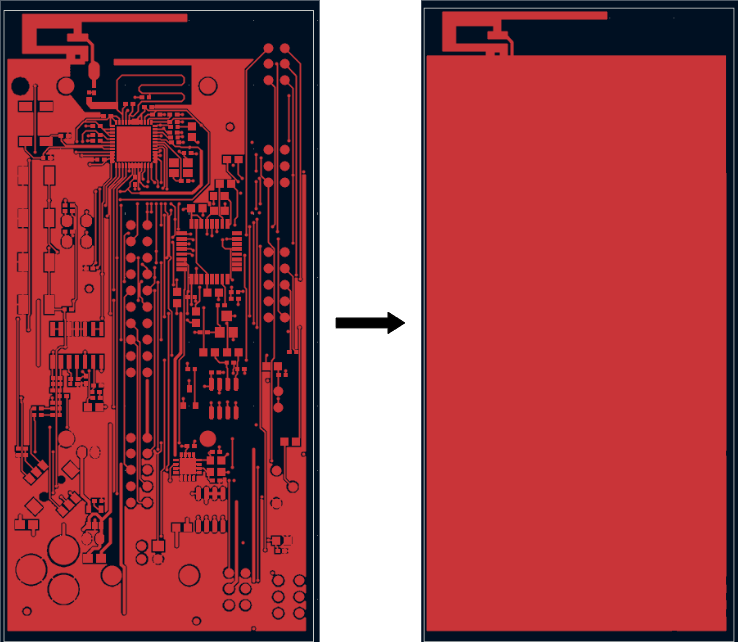
What to improve
When exporting your layout for simulation, keep only what matters for RF behavior:
- Omit decorative elements – Text, logos, and labels increase file size and they can cause compatibility issues when loading the files into CENOS RF.
- Delete unused vias and traces – Keep only the parts of the circuit involved in RF signal transmission.
- Adjust small features – Tiny copper islands or isolated pads that aren’t part of the RF path should be removed.
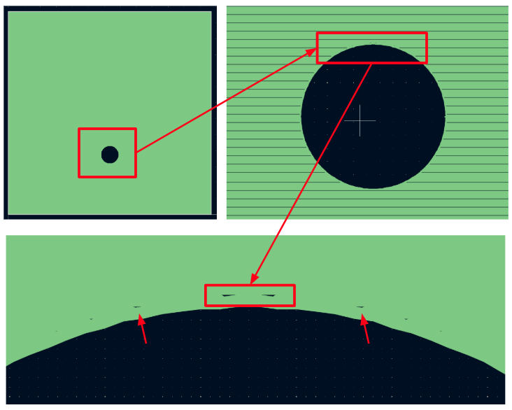
Proper geometry connections
Before importing your eCAD files into CENOS RF, it is essential to ensure that all design elements are properly connected and that the geometry is clean and continuous. Poorly defined outlines or small gaps can lead to incorrect 3D models or meshing issues.
Common geometry connection issues to avoid
- Incomplete or broken board outline
The board outline must form a closed, continuous shape. Open paths or gaps between lines can prevent correct extrusion during import. If the DRC is performed before exporting to Gerber, this type of incorrect connection is typically detected at that stage.
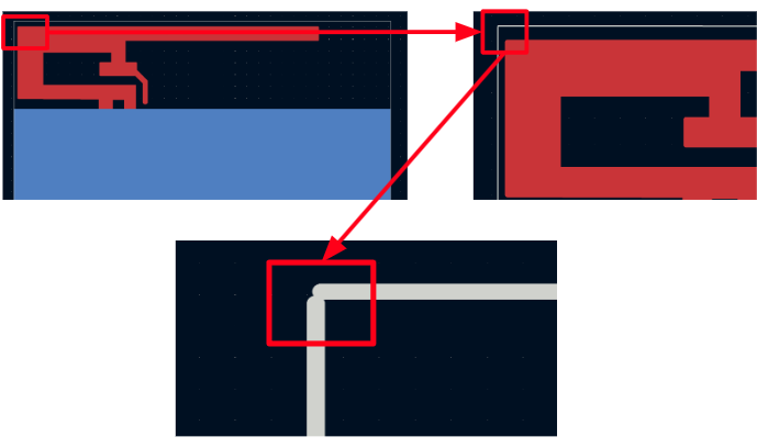
- Tiny gaps between elements
Copper areas such as ground planes or traces should be fully joined. Avoid overlapping or nearly touching shapes that aren’t truly connected in the file.
If you follow these tips for achieving good eCAD, you will have a geometry which will be easy to manipulate and mesh, and fast to calculate!
