What makes a good CAD geometry
The geometrical model of your system plays a big role in how easy or hard it will be to set up and get accurate results from a radio frequency simulation.
We have summarized the main aspects for a good, simulation-friendly CAD file, which should be followed in order to create a simple, trouble-free geometry for your simulation.
Optimize your design
Computer simulation starts with a geometrical model of the real life problem – you need to accurately depict the geometrical details to precisely calculate the physical aspects of the model. However, in most cases you can disregard some of the geometrical details, which do not have such a significant impact on the physical results, to optimize the simulation.
The following features can be deleted, as they take up a significant amount of calculation time and computer power without considerable contribution to results.
Create geometry as a single solid
In many CAD softwares it is easier to build the model from blocks, which are then combined to form a complete object CAD. When creating geometry for simulation, these blocks should be fused together to form a single solid – doing this helps remove unnecessary faces between blocks and streamlines the setup of geometric properties and the meshing process.
Delete unnecessary elements
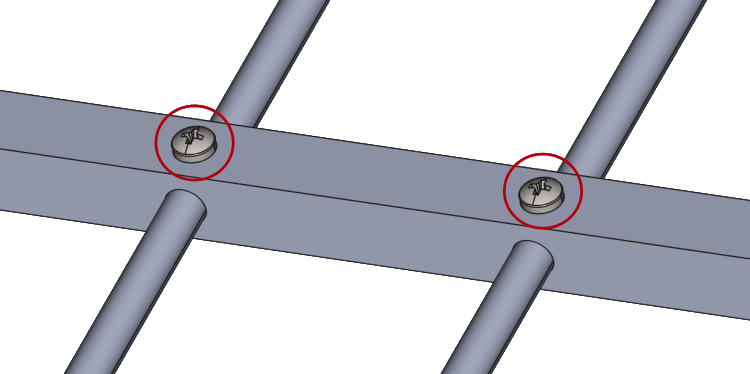
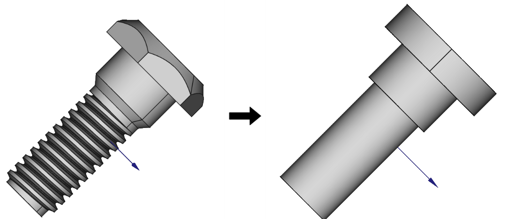
Depending on the nature of your model, one or more plastic components may be present in the design. It is important to evaluate the relevance of these components and remove them if they do not have a significant impact on the overall performance or analysis.
For example, you can
- remove plastic holders, bolts, threads, embedded text or small parts used for mechanical components
but you should
- leave any plastic encasings or covers over your geometry.
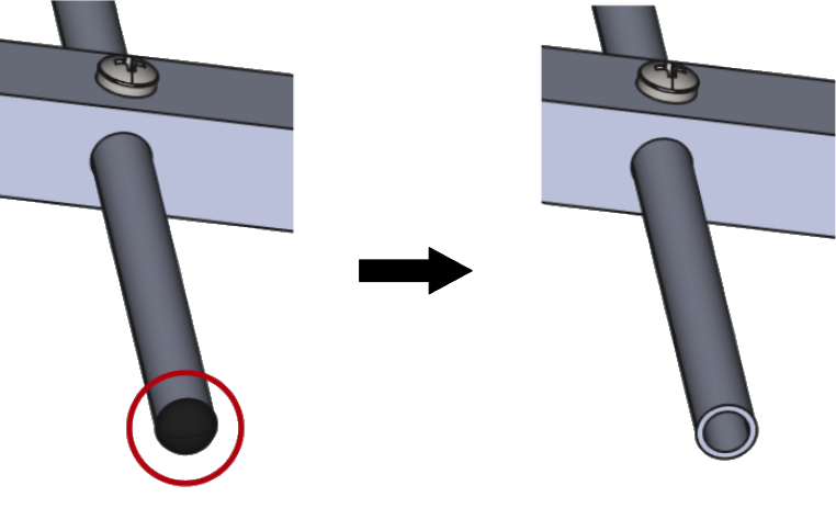
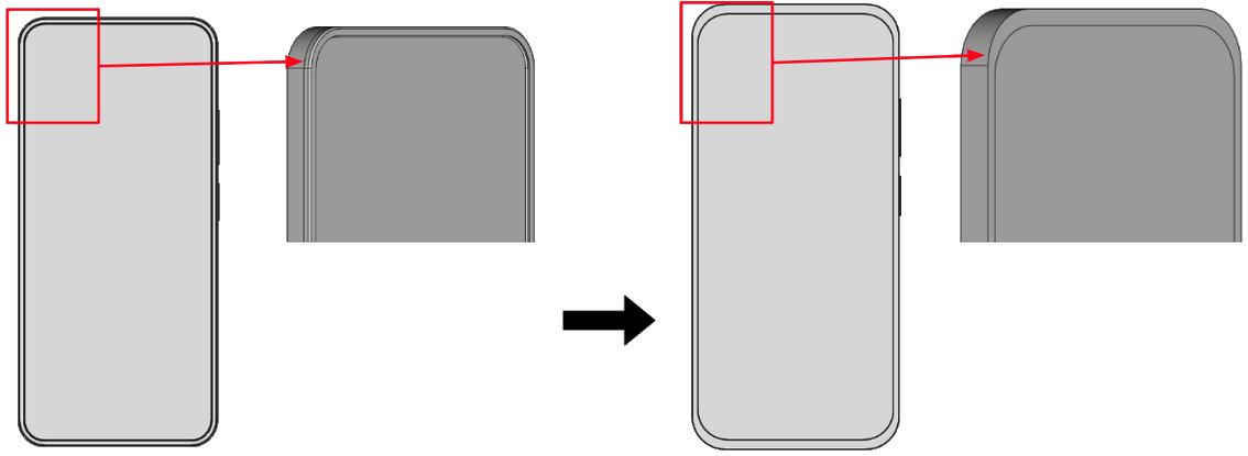
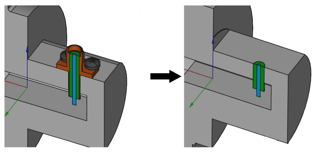
Get rid of small details
Small details have a negligible impact on the simulation results, but they take up a lot of calculation time, as they need to be resolved through mesh, which increases the mesh element count significantly. Get rid of details such as small fillets, holes and narrow gaps.
You can replace the curvatures and threads of a bolt with simple cylinders
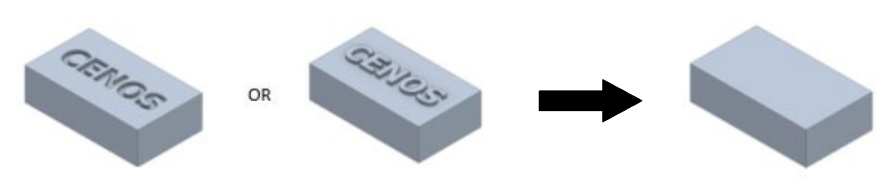
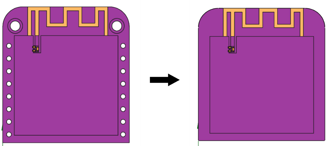
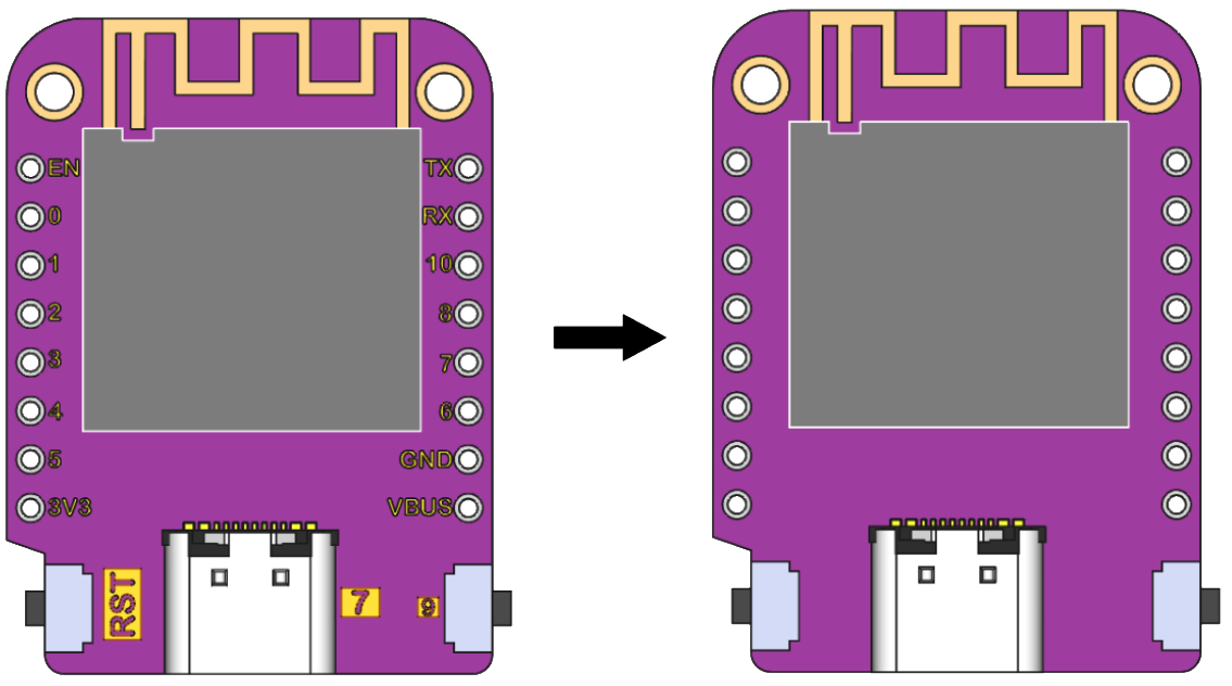
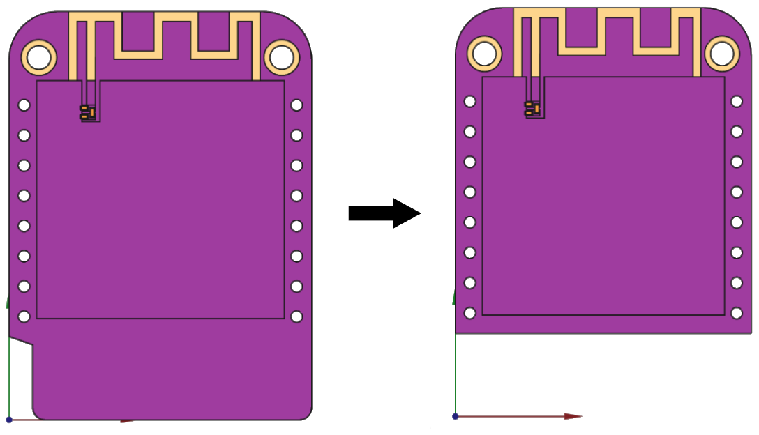
In PCB models, it is common to include silkscreen layers that provide visual and textual information that helps in the assembly and maintenance of electronic components. However, these elements are not relevant in the simulation process and can be removed.
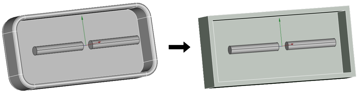
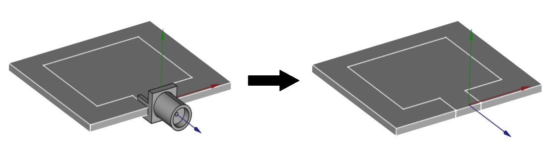
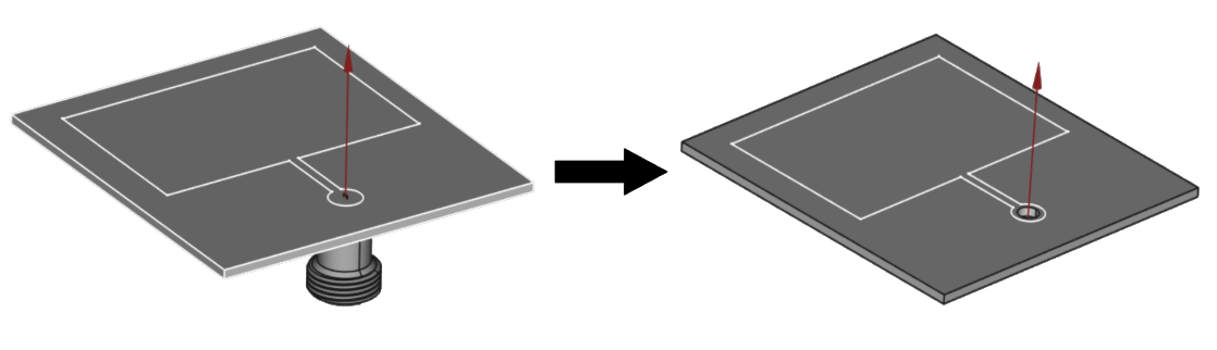
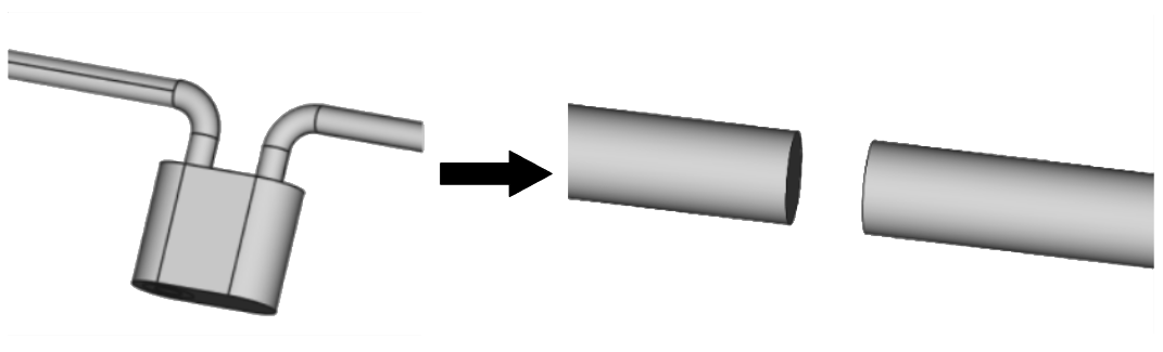
Port geometry optimization
The port or feed is one of the most important parts of the assembly, however, you can easily tailor the port geometry, to make the simulation faster without significant losses in accuracy.
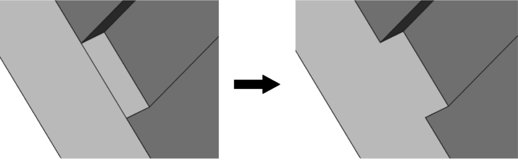
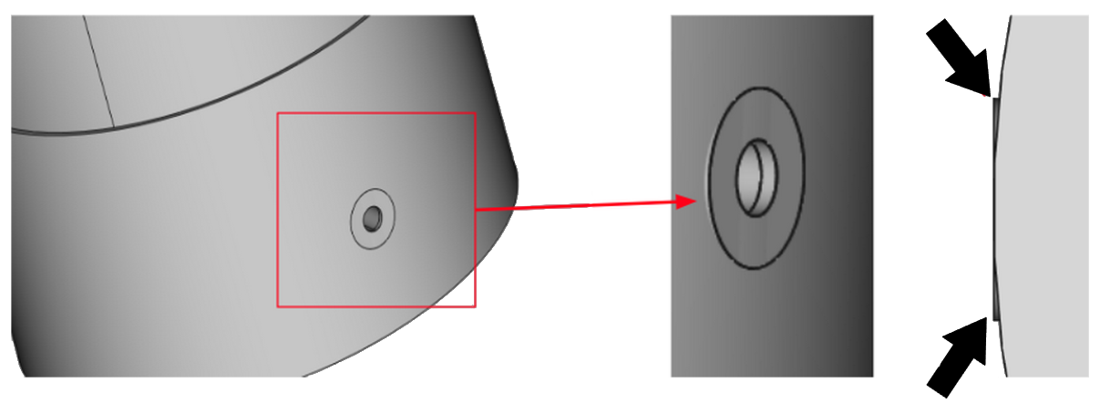
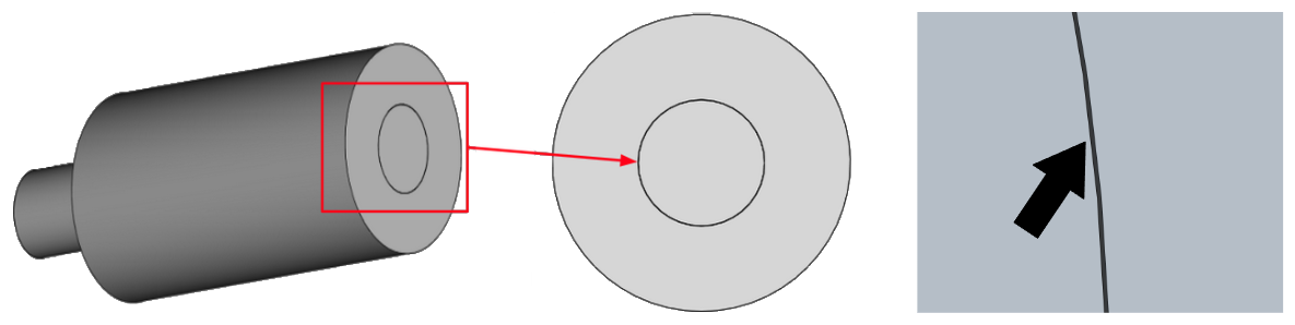
Resolve inaccurately connected geometrical parts
During geometry creation be careful with connections between different parts – inaccurate connections will result in meshing problems and calculation errors!
Overlapping
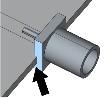
Gaps
PCB geometries
Model minimization
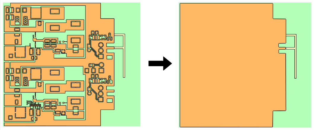
In many cases, the PCB to be simulated is used for different purposes or contains elements whose functions do not affect the primary element being simulated. In such cases, it is possible to reduce the model to include only the relevant elements.
Optimization of conductive layers
One effective way to simulate conductive layers is to reduce the geometric detail of traces and elements, using simpler shapes that preserve essential electromagnetic behavior. For instance, thin or complex traces can be replaced with wider or more basic patterns that maintain core functionality.
In many cases, certain details of the conductive layers are not relevant to RF analysis. Removing them can significantly reduce model complexity. Grouping nearby or related components into a single region can also streamline the simulation process.
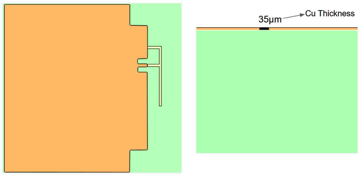
When the conductive layers are of a substantially small thickness (≤50 µm), they can be approximated as 2D surfaces rather than using the 3D layer.
Component reduction
In RF simulations, not all components on a PCB contribute equally to the behavior of the radio frequency signals. Passive components may have minimal impact on the antenna or RF part simulated. Because of this, they can often be simplified or omitted. Similarly, decorative or non-functional components, like mounting holes or mechanical supports, should be considered for removal if they do not influence the electrical performance.
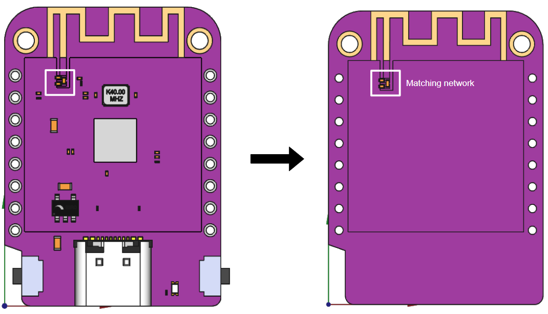
Passive components in your simulation
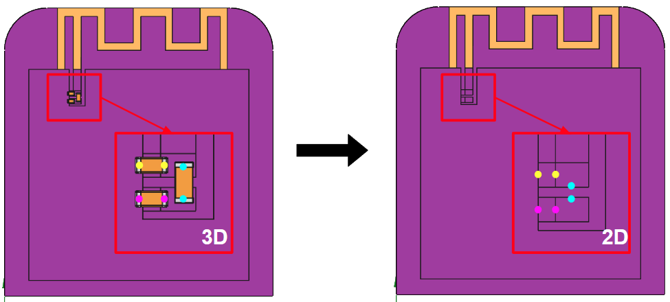
The role of passive components, such as resistors, capacitors, and inductors, is fundamental in RF circuit design. However, the 3D components can significantly increase the complexity of CAD models. In CENOS RF, such components can be simulated using lumped elements, which are assigned in the Geometry section. Therefore, in your CAD model, these components can be used as simple 2D patches.
In the following image you will see what passive components would look like without including 3D elements. Each colored dot represents one of the terminals of the lumped elements to be used to make a correct representation of these elements. Each terminal should be connected to the corresponding pad, just as it is done in the actual model.
If you follow these tips for achieving good CAD, you will have a geometry which will be easy to manipulate and mesh, and fast to calculate!
